Model

Service Hotline

0755-82564498

News Center

Introduction to common categories of fiber optic connectors
The technology in the network communication industry is constantly developing, and with the implementation of urban optical networks, in recent years, technologies such as fiber optic connectors, optical cables, and optoelectronic equipment have also seen better development and wider applications. As the core component of interconnect products, fiber optic connectors have naturally attracted people's attention. In fiber optic communication systems, the use of fiber optic connectors is also very large. It is an important connector electronic component used to connect and disconnect fiber optic signals. Below are some common fiber optic connectors:FC (F01) type fiber optic connectorThe FC type connector mainly adopts a metal threaded connection structure, and its pin body uses precision ceramic pins with an outer diameter of 2.5mm. According to the different shapes of its pin end faces, it can be roughly divided into two structures: FC/PC with spherical contact and FC/APC with oblique spherical contact. CJT connector technicians tell you that the FC type connector is currently the most widely used variety in the world and is also the main variety used in China. Two SC (F04) type fiber optic connectorThis is a molded plug-in coupled single-mode fiber optic connector, which has the same structural dimensions as the FC type, and the pin body is also a precision ceramic pin with an outer diameter of 2.5mm. In addition, its end face treatment adopts PC or APC grinding method; The fastening method is plug-in bolt type. This type of connector is inexpensive, easy to plug and unplug, with minimal fluctuations in connection losses, high compressive strength, and high installation density. Three ST type fiber optic connectorThe connector here adopts a key type bayonet locking structure (similar to BNC connection structure), and the pin body is a precision ceramic pin with an outer diameter of 2.5mm. In addition, the end face shape of the pin is usually PC surface.
Introduction to common categories of fiber optic connectors
2025-06-23 10:24:00
Science popularization and innovative design of professional application fields for board to board connectors
The widespread application of board to board connectors has emerged against the backdrop of electronic devices continuously moving towards miniaturization, integration, and high-speed development. The trend of domestic substitution of board to board connectors is becoming increasingly evident! This trend not only reflects changes in market demand, but also embodies the comprehensive role of technological progress and policy support. With the popularization and acceleration of electronic products, the requirements for connections between circuit boards are also increasing. Science popularization and innovative design of professional application fields for board to board connectors Segmented explanation of the application areas of board to board connectors:The application of board to board connectors is equally widespread. With the development of the Internet, the data center has become an important infrastructure. Board to board connectors are mainly used in data centers to connect servers, storage devices, network equipment, etc., achieving high-speed transmission and exchange of data. Due to the extremely high requirements for data transmission speed and stability in data centers, board to board connectors play a crucial role here. The field of medical instruments is also one of the important application areas of board to board connectors. With the development of medical technology, more and more medical instruments have entered households. Board to board connectors are mainly used in medical instruments to connect components such as power supply, signal transmission, and data storage, improving the safety and reliability of the instrument. For example, in an electrocardiograph, board to board connectors ensure accurate transmission and storage of electrocardiogram signals, providing doctors with accurate diagnostic basis. In addition, in remote medical systems, board to board connectors also play a key role, such as video calls, data transmission, etc., allowing patients to receive professional medical services at home, reducing medical and time costs. As an indispensable core component in modern electronic devices, board to board connectors will greatly change people's way of life and work with the promotion of 5G technology. In 5G communication systems, board to board connectors are mainly used to connect devices such as base stations, antennas, and terminals, achieving high-speed wireless signal transmission. The 5G communication system has extremely high requirements for the performance and reliability of connectors, as any minor malfunction can lead to communication interruption or data loss. Board to board connectors, with their high reliability and stability, ensure the normal operation of 5G communication systems and the accuracy of data transmission. With the rapid development of industrial automation, robots have been widely used in various production fields. Board to board connectors are mainly used in robots to connect components such as sensors, actuators, and control boards, achieving various functions of the robot. For example, in industrial robots, board to board connectors ensure accurate connection and communication between sensors and actuators, enabling the robot to perform precise operations according to preset programs. The stability and reliability of this connection method are of great significance for improving production efficiency and product quality. Precautions for using board to board connectors:Board to board connectors are divided into single slot, double slot, and side plug types, with the main characteristics of fast transmission speed, wide application range, and flexible installation. Board to board connectors need to pay more attention to details in application, otherwise it is easy to cause damage and affect the use of the product. Board to board connectors are a type of connector that generates heat during signal transmission after each insertion, resulting in loss and gradually weakening the performance of the connector. When the number of insertions and removals of board to board connectors reaches a certain level, the connector terminals will also wear out. If not maintained in a timely manner, it can lead to board to board connector failures. Qualification and Certification of Board to Board Connector Production and Wholesale SuppliersIndustry certification: Products must pass UL, CE, RoHS and other certifications to comply with international standards. Technical support: Suppliers are required to provide comprehensive services such as selection guidance, sample testing, and failure analysis. The localization of board to board connectors not only helps to reduce costs, but also promotes the independent and controllable development of the entire electronic industry chain, laying a solid foundation for the rise of Chinese manufacturing. Friendly reminder, when selecting board to board connectors, a comprehensive evaluation should be conducted from multiple dimensions such as technical parameters, application scenarios, and supplier qualifications to ensure that the product meets system requirements.
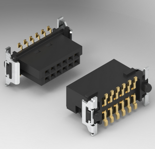
Science popularization and innovative design of professional application fields for board to board connectors
2025-06-23 10:23:00
Type-C Interface EMI Optimization: Collaborative Noise Reduction Scheme of Three Layer Shielding and Ferrite Magnetic Ring
As the core connection standard of modern electronic devices, Type-C interface has higher requirements for electromagnetic compatibility (EMI) due to its high-speed transmission and high-power charging capability. With the increase of data transmission rate, the electromagnetic radiation problem of Type-C interface under high-frequency signals is becoming increasingly prominent, which may interfere with other electronic devices and even affect its own stability. To address this challenge, the industry has proposed an EMI optimization solution of "3-layer shielding+ferrite magnetic ring", providing an innovative path for the reliability of Type-C interfaces.The EMI problem of Type-C interface mainly stems from the fast switching of high-frequency signals and current fluctuations. Under USB 3.2 or Thunderbolt 4 protocols, the operating frequency of Type-C interface can reach tens of GHz, and crosstalk and common mode noise between signal lines are easily radiated to the external environment through cables. The traditional single-layer shielding design is difficult to completely suppress high-frequency radiation, while the "3-layer shielding" scheme significantly improves shielding effectiveness through a multi-layer isolation structure. The first layer of shielding covers the outer layer of the cable, blocking external interference; The second layer wraps the internal wire pairs to reduce signal crosstalk; The third layer provides independent shielding for power lines to prevent magnetic field leakage caused by high currents. This layered design gradually blocks the propagation path of electromagnetic radiation, reducing the EMI index of Type-C interface by more than 40%. The shielding effectiveness of Type-C interface needs to be further optimized by combining with ferrite magnetic rings. Ferrite magnetic rings are integrated into interface terminals or cables to suppress common mode noise through their high-frequency impedance characteristics. When high-frequency current passes through the Type-C interface, the magnetic ring absorbs electromagnetic energy in a specific frequency band and converts it into thermal energy for dissipation. For example, in the range of 10MHz to 1GHz, ferrite magnetic rings can attenuate common mode interference by more than 20dB. This dual mechanism of "active absorption+passive shielding" enables the Type-C interface to maintain a stable electromagnetic environment even during high-speed transmission above 5Gbps.The 3-layer shielding design of Type-C interface poses higher requirements for manufacturing processes. Each layer of shielding material needs to balance conductivity and flexibility, such as using a combination of aluminum foil Maillard layer, woven copper mesh, and polymer composite material. The aluminum foil layer provides basic shielding, the copper mesh enhances structural strength and expands shielding coverage, while the polymer material ensures the bending life of the cable. At the same time, the selection of ferrite magnetic rings needs to accurately match the operating frequency of the Type-C interface to avoid a decrease in filtering effect due to impedance mismatch. This refined design enables the Type-C interface to meet both the 40Gbps transmission requirements of USB4 and pass strict electromagnetic certification tests such as FCC and CE.The EMI optimization solution for Type-C interface is driving the upgrade of industry standards. The International Electrotechnical Commission (IEC) has included multi-layer shielding in the new version of the USB cable design guidelines, and the application of ferrite magnetic rings has also been included in the recommended specifications for some high-speed connectors. In the field of consumer electronics, manufacturers such as Apple and Samsung have adopted similar solutions in the Type-C interface of their flagship devices; In industrial scenarios, the vehicle mounted Type-C interface successfully addresses the electromagnetic interference challenge of high-voltage systems in electric vehicles through a "3-layer shielding+dual magnetic ring" design. These practices have shown that this solution not only enhances user experience, but can also be extended to more demanding application environments. The EMI control technology of Type-C interface will develop towards integration and intelligence in the future. With the introduction of new technologies such as silicone encapsulation shielding layers and nano magnetic materials, the shielding structure of Type-C interfaces may further become thinner and lighter while maintaining or even improving performance. In addition, the intelligent magnetic ring can adapt to the noise suppression requirements of different frequency bands by dynamically adjusting its impedance characteristics. This technological evolution will enable the Type-C interface to continuously meet the stringent EMI requirements of 6G communication and AI computing devices for high-speed connectors while maintaining a compact size. Through material innovation and design optimization, the Type-C interface will continue to consolidate its leading position as a universal connectivity standard.
Type-C Interface EMI Optimization: Collaborative Noise Reduction Scheme of Three Layer Shielding and Ferrite Magnetic Ring
2025-06-23 10:19:00
Special waterproof Type-C for deep-sea equipment: 20MPa pressure chamber tested 1000 times without failure after plugging and unplugging
The application of Type-C interface in deep-sea devices is becoming an important breakthrough in the field of underwater technology. With the rapid development of ocean exploration and deep-sea exploration equipment, the reliability issues of traditional connectors in high-pressure, high salt, and high humidity environments are becoming increasingly prominent. In response to this challenge, the waterproof Type-C interface specifically designed for deep-sea equipment has achieved excellent performance without failure after 1000 insertions and removals in a 20MPa pressure chamber through innovative sealing design and material technology, providing a stable and durable connection solution for underwater equipment.The deep-sea waterproof performance of Type-C interface is primarily attributed to the multi-layer composite sealing structure. Through the integrated design of silicone sealing rings, nano coatings, and metal shells, the interface can still isolate seawater infiltration under extreme pressure. In the 20MPa pressure chamber simulation test, the sealing layer of the waterproof Type-C interface dedicated to deep-sea equipment can withstand external pressure equivalent to a depth of 2000 meters, while maintaining the integrity of signal transmission. This design not only solves the problem of aging of traditional rubber seals, but also extends the service life of the interface in salt spray environments through the anti-corrosion treatment of the metal shell.The mechanical durability of Type-C interface is another key indicator for deep-sea equipment applications. In 1000 cycles of insertion and extraction testing, the metal contacts of the interface are coated with gold and have an elastic self-cleaning structure to ensure low resistance connection even after repeated insertion and extraction. The test data shows that even after thousands of insertions and removals, the change rate of contact resistance is less than 5%, and the signal attenuation is controlled within 3dB. This breakthrough in performance enables the specialized waterproof Type-C interface for deep-sea equipment to handle long-term deployment and frequent maintenance of marine research tasks, such as applications in underwater robots, underwater observation stations, and other scenarios. The high voltage tolerance of Type-C interface cannot be achieved without precise structural simulation and material testing. The R&D team optimized the stress distribution of the interface through finite element analysis to avoid sealing failure caused by shell deformation under 20MPa pressure. At the same time, the shell material is a composite structure of titanium alloy and PEEK (polyetheretherketone), which balances lightweight and compressive strength. In the actual testing of the pressure chamber, no cracks or deformations occurred at the interface under extreme pressure, verifying the reliability of its structural design. This dual verification mode of "simulation+actual testing" provides technical support for the engineering application of waterproof Type-C interfaces specifically designed for deep-sea equipment. The electrical performance of Type-C interface has also been tested in deep-sea environments. By incorporating ferrite magnetic rings and double-layer shielded cables, the interface can effectively suppress electromagnetic interference (EMI) even in high voltage environments. Tests have shown that under a pressure of 20MPa, the transmission rate of the interface can stably support the 10Gbps standard of USB 3.2 Gen2, with an error rate of less than 1 × 10? 12. This performance enables it to meet the bandwidth requirements of scenarios such as underwater high-definition cameras and sonar data transmission, laying the foundation for the intelligent upgrade of deep-sea exploration equipment.The deep-sea adaptability of Type-C interface is driving the innovation of industry standards. The International Marine Engineering Association (IMCA) has included this type of interface in the "Technical Guidelines for Underwater Equipment Connectors", and its testing standards have been adopted by multiple research institutions. In commercial applications, Norwegian deep-sea robot companies have adopted waterproof Type-C interfaces in bulk to replace traditional wet plug connectors, reducing operation and maintenance costs by 40%; The Chinese "Jiaolong" scientific research team has also verified its reliability in experiments. In the future, with the development of emerging fields such as deep-sea oil and gas development and underwater data centers, the high-pressure waterproof technology of Type-C interface is expected to become a universal connection standard for underwater equipment.The technological evolution of Type-C interface will continue to focus on performance breakthroughs in extreme environments. For example, improving the oxidation resistance of contacts through graphene coating, or using intelligent sealing materials to achieve pressure adaptive dynamic sealing. These innovations will enable the specialized waterproof Type-C interface for deep-sea equipment to remain stable in deeper waters (such as the Mariana Trench) and more complex working conditions, providing stronger technical support for human exploration of ocean mysteries.
Special waterproof Type-C for deep-sea equipment: 20MPa pressure chamber tested 1000 times without failure after plugging and unplugging
2025-06-23 10:15:00
Big data analysis of JSSC, a top tier journal in chip design: none of the top 50 Chinese companies with institutional contributions made it onto the list! Several chip companies from the United States and South Korea have entered the top ten
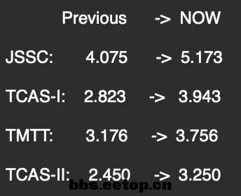
1.Overview of Journal Citation ReportsThe latest Journal Citation Reports (JCR) have been released, and the impact factors of microelectronics related journals have been significantly improved. Among them, JSSC, a top tier journal, achieved an impact factor of over 5 for the first time (reaching 5.173), while TCAS-I surpassed TMTT and came in second place. TCAS-II also entered the 3-point range for the first time.At present, the journals (Q1) of Electrical and Electronic Engineering (Engineering, Electrical&Electronics) in the JCR division (non Chinese Academy of Sciences division) are JSSC (rank: 33), TCAS-I (rank: 57), and TMTT (rank: 61). (Note: One of the requirements for Shenzhen Peacock Plan Class C (1.6 million) is to publish three JCR Q1 journals.). ) Figure 1. Impact factor ranking of microelectronics related journals, JSSC ranks first with 5.1732. JSSC influencing factorsBelow we will analyze the relevant data of JSSC in detail. Figure 2 shows the specific calculation formula for the JSSC impact factor in 2018. It refers to the number of JSSC papers cited in 2017 and 2016 (2716) divided by the total number of papers published in 2017 and 2016 (525) throughout 2018. Figure 2 JSSC Impact Factor Calculation Formula3. Reasons for the significant increase in JSSC's impact factor in 2018As shown in Figure 3, among the top 7 papers with the highest number of applications in 2018, AI papers published by MIT's Sze research group contributed 111 citations, far higher than JSSC papers later on. The remaining highly cited papers mainly focus on 5G phased array, Internet of Things, etc. This also reflects the current era background of artificial intelligence (AI), 5G millimeter wave communication, and 5G Internet of Things. In the foreseeable years, these topics will still be key to improving the JSSC impact factor. It is worth mentioning that the 77G phased array automotive radar JSSC, developed by the research group of Wang Zhihua and Chi Baoyong from Tsinghua University in China, ranks fourth in highly cited papers. Which countries have contributed to JSSC? As shown in Figure 4, the contribution of the United States to JSSC is in an absolute leading position, even higher than the sum of the countries ranked 2-9 behind. This reflects the absolute dominance of the United States in chip design, and is also the reason why the United States dares to impose chip embargo and technology blockade on Huawei and ZTE companies in China without restraint. After decades of continuous struggle, Chinese Mainland's contribution to JSSC has reached the third place, lower than that of South Korea and slightly higher than that of Japan/Netherlands. Taiwan, on the other hand, ranks sixth. Among the top ten countries and regions, Asian countries and regions account for 5 places, with South Korea ranking second, reflecting the broad prospects of integrated circuit design in Asia. 5. Which institutions have contributed to JSSC? Figure 5 shows the top 50 universities or companies contributing to JSSC. The University of California System and Intel are listed as the top contributing universities and companies, respectively. In terms of the company, well-known chip companies such as Intel, Broadcom, Qualcomm, and Samsung are all ranked in the top ten. Unfortunately, Chinese chip design companies did not make the list. In recent years, the University of Macau in China has experienced rapid development in microelectronics, ranking 13th on the JSSC contribution list. The Hong Kong University of Science and Technology ranks 22nd. Only Tsinghua University from mainland China made the list, tied for 41st place. In Taiwan, China, Hsinchu Tsinghua University and National Jiaotong University are on the list. It can be seen that the University of Macau has become the most shining star in microelectronics design in Greater China. This list can also serve as a guide for students who want to study microelectronics abroad to choose schools. 6. ConclusionAs the top tier journal in integrated circuits, JSSC's big data analysis can accurately reflect trends in integrated circuits. The JSSC papers on AI and 5G have become popular, increasing the impact factor of JSSC and indicating the development direction of integrated circuits in the coming years. The JSSC regional contribution ranking shows that Chinese Mainland has made great progress in the field of integrated circuit design after decades of efforts, but it is still far from the United States, even compared with South Korea. In terms of universities, the University of Macau, the Hong Kong University of Science and Technology, and Tsinghua University have all entered the JSSC list, demonstrating the strength of China's scientific research field. Among them, the University of Macau has shone brightly in recent years. In the future, we hope that more universities and chip design companies from mainland China can enter the JSSC list.
Big data analysis of JSSC, a top tier journal in chip design: none of the top 50 Chinese companies with institutional contributions made it onto the list! Several chip companies from the United States and South Korea have entered the top ten
2025-06-23 10:09:00
35.4 billion yuan! Gaota Semiconductor's shareholders' meeting approves its acquisition by Intel
In order to revive its semiconductor leadership position, Intel is currently investing billions of dollars to build its own wafer fabs and expanding its wafer foundry business. In February, it announced a $5.4 billion (35.4 billion RMB) acquisition of Israel's Tower Semiconductor, which has now been approved by its shareholders.According to reports, Tower Semiconductor announced that its shareholders' special meeting has approved the agreement to sell the company to Intel, and both parties need to obtain all necessary regulatory approvals before the transaction is completed.Until the completion of the transaction, Intel's Manufacturing Services Division (IFS) and Tower Semiconductor will operate independently. During this period, Intel's Manufacturing Services Division (IFS) will continue to be led by Thakur, while Tower Semiconductor will continue to be led by Ellwanger.After the transaction, Intel aims to make these two organizations a fully integrated foundry business. At that time, Intel will share more details about the integration plan.It is reported that Gaota Semiconductor Co., Ltd. is a semiconductor professional OEM factory in Israel, headquartered in Migdal Emek, Israel.The company currently operates only one 6-inch wafer fab (process between 1 micron and 0.35 microns) and one 8-inch wafer fab (process between 0.18 microns and 0.13 microns) in Israel, with one 8-inch wafer fab each in California and Texas, providing process services for 0.18 microns (Texas plant) and 0.18 to 0.13 microns (California plant).Gaota Semiconductor ranks seventh in the global wafer foundry market, with an annual revenue of approximately 1.3 billion US dollars. Although its scale is not large, it is in a leading position in special processes and ranks first in the field of analog chip foundry. Its RF and high-performance analog circuit technologies can support a wide range of high-speed, low-power products for consumer, industrial facility, and automotive electronics applications.
35.4 billion yuan! Gaota Semiconductor's shareholders' meeting approves its acquisition by Intel
2025-06-23 10:04:00
How to use the buzzer without breaking
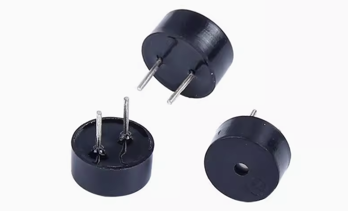
Many users focus on comparing prices when purchasing buzzers, while ignoring the electrical performance parameters of the buzzer, which can easily cause mismatches between the buzzer and the PCB drive circuit, leading to various quality issues. Matching the buzzer with the PCB circuit is the longest and least likely way for the buzzer to last. In addition, during use, the following precautions should be taken: 1.Excessive welding temperature can easily cause deformation of the buzzer shell, loose pins, and result in no or low sound; 2.The starting voltage of the buzzer is too low or too high, which may result in low or sandy sounds during use; 3. After being stored for a period of time, the buzzer produces a low sound, but after using it for a period of time, it becomes normal. This situation may be due to the influence of a humid environment on the buzzer, and attention should be paid to moisture prevention.4. When the buzzer works on the PCB board, it may experience pitch changes or no sound, but there is no problem when tested individually. This situation may be caused by magnetic field interference on the buzzer.
How to use the buzzer without breaking
2025-06-23 09:55:00
Will USB Type-C interfaces be replaced by contactless alternatives?
Although device manufacturers in the market are attracted by the compact size, support for multiple protocols, and power management capabilities of Type-C connectors, their market adoption rate is continuing to rise. However, it cannot be ignored that most current Type-C implementations, especially in mobile devices, only use it to transmit electrical energy and data at lower speeds. In addition, it is difficult to manage RFI/EMI emissions from connectors and cables at high data rates, which can interfere with Wi Fi signals.The new non-contact solution can achieve the main advantages of mechanical USB Type-C connectors without any mechanical connectors, including multi protocol support for high-speed data transmission, streaming of high-resolution video files, and management capabilities for fast charging protocols for USB power input and output between devices. In addition, this non-contact connector also supports various low-speed protocols, including I2C and GPIO, which are not currently supported by mechanical Type-C connectors. The solution can transfer data at very high speeds, such as USB SuperSpeed and FullSpeed, without causing interference issues, making it extremely efficient for transferring large files between mobile devices.The industry has already experienced the first strong growth of Type-C connectivity technology in the market, and it is expected that this non-contact solution will become an attractive option. ”Zhang Jinfan said, 'This new plan is expected to be available to customers by the end of the fourth quarter.'.”The new non-contact USB Type-C alternative solution includes Keyssa's Kiss Connectors connector, which is a small and low-power solid-state connector. Meanwhile, F-One technology is a highly integrated aggregation controller product series that can be used to flexibly aggregate various communication protocols into the same F-One serial channel.
Will USB Type-C interfaces be replaced by contactless alternatives?
2025-06-23 09:53:00
Added to cart